Nanowires
Semiconductor nanostructures provide powerful ways to engineer electronic and optical properties by confining carriers at the nanometer scale. Structures such as quantum dots, nanowires, and superlattices allow precise control of carrier confinement, emission wavelength, and optical coupling, enabling new generations of infrared optoelectronic and quantum photonic devices.
A major focus of our research is the development of quantum dots formed by liquid droplet epitaxy (LDE). In this growth method, metallic droplets are first deposited on the semiconductor surface and subsequently crystallized to form nanoscale semiconductor islands or nanohole structures. This approach enables flexible control over dot geometry, composition, and density, and is particularly attractive for creating quantum dots in material systems that are difficult to realize using conventional self-assembled growth.
LDE quantum dots provide strong three-dimensional carrier confinement and narrow optical linewidths, making them promising candidates for infrared emitters, single-photon sources, and quantum photonic devices. In our work we explore the use of antimonide and related III–V material systems to extend quantum-dot emission toward the mid-infrared, where semiconductor quantum light sources remain largely unexplored.
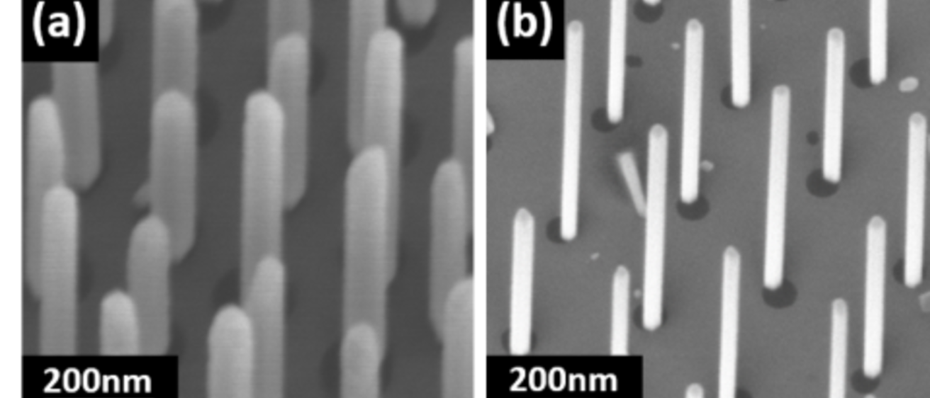
In addition to quantum dots, we investigate other semiconductor nanostructures that provide complementary approaches to controlling carrier dynamics and light-matter interactions. Semiconductor nanowires offer one-dimensional confinement and can serve as integrated optical cavities and waveguides, while superlattice heterostructures allow precise band-structure engineering through periodic stacks of thin semiconductor layers.
By combining epitaxial growth, nanofabrication, and optical spectroscopy, our group studies both the fundamental physics and device applications of these nanostructures. Current research directions include:
- Liquid droplet epitaxy quantum dots for infrared emitters and single-photon sources
- Coupled quantum dots and multi-color photon emission for sensing and quantum networks
- Nanowire and nanostructured photonic devices
- Superlattice heterostructures for infrared optoelectronics
These nanostructured materials provide a versatile platform for exploring new approaches to infrared photonics, sensing, and quantum optical technologies.