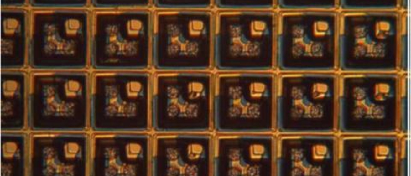
Two color SLED array
Mid-Infrared Optoelectronics
Mid-infrared optoelectronics involves semiconductor devices that generate and detect light at wavelengths from roughly 2–12 μm. This spectral region contains strong molecular vibrational resonances and is therefore critical for applications in chemical sensing, environmental monitoring, medical diagnostics, thermal imaging, and defense technologies. Mid-infrared devices are typically based on compound III–V semiconductor materials such as antimonide alloys and superlattice heterostructures.
Our research focuses on developing new infrared emitters and detectors using epitaxially grown semiconductor heterostructures. A central challenge in mid-infrared optoelectronics is that as semiconductor bandgaps narrow, device efficiency is often limited by nonradiative processes such as Auger recombination and Shockley–Read–Hall scattering. Our work explores new materials, structures, and photonic engineering approaches to overcome these limitations.
Key research directions include:
- Superlattice-based mid-infrared emitters and detectors, including cascaded LED architectures and high-efficiency W-superlattice light sources.
- Large-format infrared LED arrays for applications such as thermal scene projection and active infrared illumination.
- Photonic engineering of infrared devices, including microcavities, metastructures, and nanostructured surfaces to enhance light extraction and radiative efficiency.
- Quantum-dot and nanostructured emitters for emerging applications in infrared sensing and quantum photonics.
By combining molecular beam epitaxy growth, micro- and nanofabrication, and optical characterization, our group studies both the fundamental physics and practical device engineering needed to create more efficient and scalable infrared photonic technologies.
High-Efficiency Mid-Infrared Superlattice LEDs
Compound Semiconductor Innovation and Antimonide Infrared Emitters (PDF of Presentation)