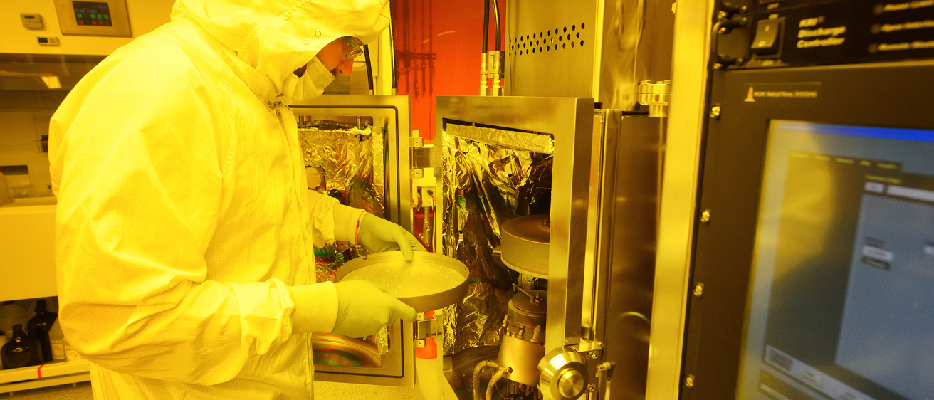
The Materials Analysis, Testing, and Fabrication (MATFab) Facility Located in the IATL
Credit/Provider: Justin Torner - Staff Photographer - The University of Iowa
Micro and Nanofabriction
Micro- and nanofabrication provide the tools needed to transform semiconductor materials into functional photonic and electronic devices. These techniques, originally developed for integrated circuit manufacturing, allow structures to be patterned with dimensions ranging from micrometers down to tens of nanometers using processes such as photolithography, thin-film deposition, and plasma etching.
In our research, micro- and nanofabrication are used in the University of Iowa MATfab facility to create semiconductor devices and photonic structures that control the generation, propagation, and detection of light in the infrared. By precisely shaping materials and interfaces, fabrication enables new device architectures that would not be possible using materials growth alone.
Our group combines standard semiconductor processing methods with custom device fabrication to develop structures such as:
Infrared emitters and detectors, including mesa devices and integrated emitter arrays
Nanostructured photonic surfaces that enhance light extraction and optical coupling
Micro- and nanoscale resonators and cavities for controlling emission and absorption
Photonic structures integrated with quantum dots and superlattices
These devices are fabricated using a range of techniques including photolithography, thin-film deposition, dry and wet etching, and metallization. By integrating microfabrication with epitaxial materials growth and optical characterization, our work links materials synthesis, device physics, and photonic system design.
This capability allows us to explore new semiconductor device concepts while also developing practical technologies for infrared sensing, imaging, and quantum photonics.