Gen20 Molecular Beam Epitaxy
Molecular Beam Epitaxy
Molecular beam epitaxy (MBE) is a technique for growing high-quality crystalline semiconductor materials with atomic-scale control. In an MBE system, beams of atoms or molecules are generated from heated sources in an ultrahigh-vacuum environment and directed toward a heated crystalline substrate, where they condense and form epitaxial layers. Because the growth takes place in extremely clean vacuum conditions and at relatively slow rates, MBE enables precise control of layer thickness, composition, and doping at the level of individual atomic layers.
This level of control makes MBE one of the most powerful tools for creating semiconductor heterostructures, including quantum wells, superlattices, and quantum dots. These structures allow researchers to engineer electronic and optical properties in ways that are not possible in bulk materials and form the basis of many modern optoelectronic and quantum devices.
Our group uses molecular beam epitaxy to grow compound semiconductor materials for infrared photonics. A major focus is the growth of III-V antimonide semiconductor systems, which enable light emission and detection in the near-, short-, mid-, and long-wave infrared. By precisely controlling layer thickness and composition, we create complex heterostructures such as superlattices, cascaded emitter structures, and quantum-confined nanostructures.
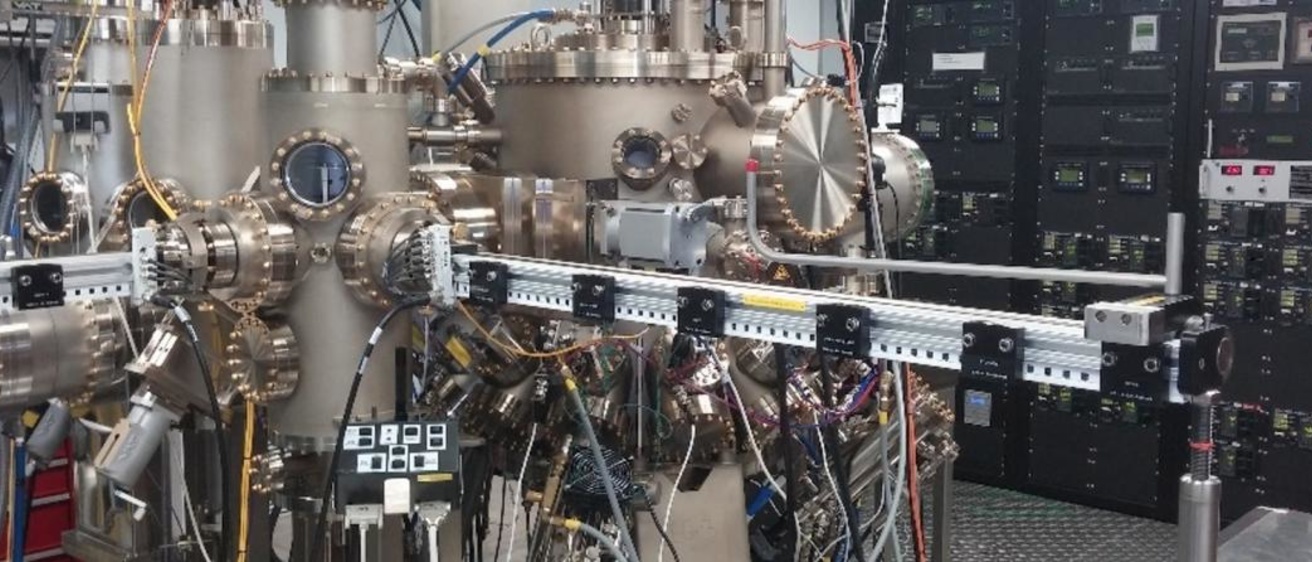
The MBE facility in the Iowa Advanced Technology Laboratories supports research across multiple groups and projects. Using this platform we develop new materials for:
- infrared emitters and detectors
- quantum-confined semiconductor nanostructures
- nanostructured photonic devices
- advanced sensing and quantum photonic systems
By combining epitaxial materials growth with microfabrication and optical characterization, our work links materials synthesis, device physics, and photonic system design to advance the next generation of infrared optoelectronic technologies.
The Art and Science of Molecular Beam Epitaxy and the Nobel Prize for Blue LEDs